NVIDIA, SK Hynix: CPO Is a Must-Win!
Both SK Hynix and NVIDIA are aggressively deploying Co-Packaged Optics (CPO) technology. SK Hynix published a research paper proposing a roadmap and performance targets for optical interconnects supporting next-generation AI systems, while NVIDIA announced that its first mass-production-ready 200G/lane CPO switch has entered full-scale production, aiming to improve network power efficiency and build large-scale AI infrastructure
Recently, the semiconductor industry has been heated up by one word—CPO. NVIDIA, which holds the key to computing power, and SK Hynix, which controls the lifeline of memory, have both rarely shown such urgency simultaneously.
SK Hynix and NVIDIA Double Down on CPO
Recently, SK Hynix and its global research team published a paper in Nature Electronics. The paper explores the development of Co-Packaged Optics (CPO) for high-performance computing and artificial intelligence, points out key technical challenges, and outlines the development trajectory of next-generation optical interconnect technologies.
Seung-Hoon Hong, head of SK Hynix's AI Infrastructure Team, and Professor Kyu-Sang Lee from the Department of Electrical and Computer Engineering at the University of Virginia (UVA), served as corresponding authors, leading a study in collaboration with researchers from the University of Illinois Urbana-Champaign (UIUC), Nanyang Technological University (NTU), the Massachusetts Institute of Technology (MIT), and Yonsei University.
From a broader perspective, the paper proposes a comprehensive technology roadmap detailing how memory, advanced packaging, and Optical Compute Interconnect (OCI) should co-evolve to support next-generation AI systems. Crucially, it also demonstrates how SK Hynix is going beyond HBM innovation to help define the architecture of next-generation AI infrastructure at the system level.
Meanwhile, the researchers set clear technical targets for next-generation AI infrastructure, including bandwidth exceeding 100 Tb/s per node, energy consumption below 1 pJ/bit, and chip-to-chip latency of less than 10 nanoseconds. The paper also presents a comprehensive technology roadmap outlining the evolution from configurations based on 2D and 2.5D interposers to 3D heterogeneous stacking, as well as the key technical challenges that must be addressed for commercial deployment.
Coincidentally, on August 14, NVIDIA officially announced that its SpectrumX Ethernet Photonics Co-Packaged Optical Switch had entered full-scale production, targeting AI factories to build next-generation scalable network infrastructure. This is the world's first mass-production-ready 200G/lane Co-Packaged Optical Switch system. According to official NVIDIA data, compared to traditional pluggable optical module solutions, it achieves a 5x improvement in network power efficiency and a 5x increase in uninterrupted runtime for AI applications, while extending the Mean Time Between Failures (MTBF) by 10 times, significantly addressing the power consumption and reliability shortcomings of ultra-large-scale AI cluster networks.
The fact that CPO has suddenly become a shared bet for both SK Hynix and NVIDIA is no coincidence. There is only one driving force behind this: data centers can no longer cope.
Data Centers Need CPO
The earliest generation of data centers extensively used Direct Attach Copper (DAC) cables for internal interconnects. Switch chips connected to DAC cables via OSFP and QSFPDD connectors, completing short-distance transmission using purely electrical signals. The advantages of copper cable solutions are prominent: low cost, simple deployment, no need for optoelectronic conversion components, and controllable power consumption in short-distance scenarios. However, the drawbacks are equally fatal. Under high-speed signals, copper wires suffer from severe attenuation, with transmission distances mostly limited to a few meters. As bandwidth increases, power consumption rises rapidly, making it completely unsuitable for high-density, ultra-high-bandwidth AI computing clusters. Consequently, it is gradually being replaced by optical interconnects.
Subsequently, the industry fully entered the era of pluggable optical modules, which remains the mainstream state of the industry today.
Switch chip boards connect to independent pluggable optical transceiver modules via OSFP and QSFPDD connectors, and then complete long-distance signal transmission through fiber optics. The biggest advantage of pluggable optical modules is flexibility: they support hot-swapping, allowing business recovery by simply replacing the module after a failure, and upgrades are convenient. Their standardized form factor fits most cloud providers' data centers. However, the shortcomings of this architecture are infinitely amplified in ultra-high-bandwidth AI clusters: there is still a centimeter-level high-speed electrical trace between the switch chip and the panel-mounted optical module. Signal loss and crosstalk occur during high-speed signal transmission. To compensate for signal loss, Retimers and equalizers inside the optical modules continuously consume power, keeping the overall network power consumption high.
For ordinary internet data centers, 800G and 1.6T pluggable optical modules are still sufficient. However, facing AI training clusters with hundreds of thousands of cards, where switch ports number in the tens of thousands, the additional power consumption and signal loss from stacking numerous ports become a heavy burden on the entire computing cluster. Traditional pluggable architectures are beginning to hit physical ceilings.
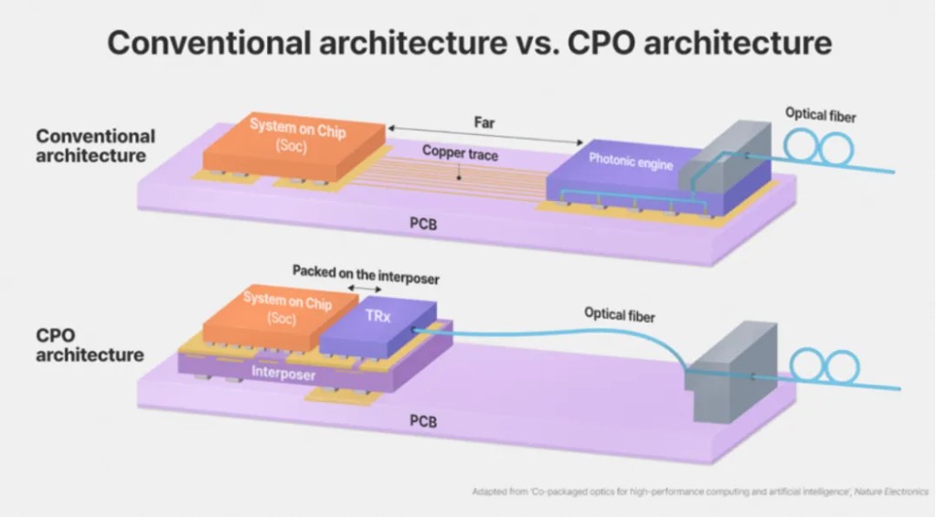
CPO was born precisely to resolve this contradiction. The CPO architecture moves the electro-optical conversion process inside the chip package, compressing the high-speed electrical signal transmission distance to a few millimeters. This avoids signal loss caused by long-distance high-speed copper traces and eliminates some DSP signal processing overhead, achieving comprehensive optimization of power consumption, latency, and reliability.
Before 200G/lane, What Was CPO Using?
However, with the release of NVIDIA's 200G/lane CPO Ethernet switch, many readers' first reaction was confusion: Isn't the industry already talking extensively about 800G and 1.6T optical modules? Is NVIDIA lagging behind by only releasing 200G? What is the difference between CPO and traditional pluggable optical modules? What does this mean for the thriving domestic optical module companies?
To answer these questions, we must first clarify a set of easily confused concepts: 200G/lane describes the rate of a single optical lane, while 800G and 1.6T refer to the total rate per port. They are not in the same dimension.
The formula for the total rate of an optical module port is: Total Rate = Single Lane Rate × Number of Lanes. The number of lanes is typically a power of 2, such as 4, 8, or 16. Here are a few common industry examples: 8×50G=400G, 8×100G=800G. Therefore, 200G/lane is not a backward new technology; rather, it is the underlying physical foundation for next-generation high-speed interconnects.
Before the mass production of 200G/lane was achieved this time, technical exploration in the CPO industry had long stagnated at 50G/lane and 100G/lane. So why must the industry push the single-lane rate to 200G/lane? The root cause lies in the underlying network pressure brought by the explosion of AI computing power.
As GPU architectures iterate from Hopper to Blackwell, and evolve towards the future Rubin architecture, the external communication bandwidth of a single GPU has seen explosive growth. Today, large AI training clusters often deploy hundreds of thousands or even millions of GPUs, requiring switches to carry unprecedented total switching capacities. If the industry remained at 100G/lane, achieving a total switch capacity of 102.4T would require doubling the number of physical lanes. The direct consequence would be a drastic expansion of switch chip area, PCB circuit board routing density hitting physical limits, and overall power consumption spiraling out of control, making cabinet power supply and heat dissipation unmanageable. The old path of simply stacking more lanes is no longer viable.
The essence of CPO (Co-Packaged Optics) is to break the traditional architecture of "separate switch chips and optical modules" that has persisted for years. It co-packages the optical engine—including lasers, modulators, and detectors—with the ASIC switch chip on the same substrate. This compresses the electrical signal transmission path from centimeters in traditional solutions to millimeters, fundamentally solving the power consumption, signal attenuation, and bandwidth bottlenecks of traditional interconnect architectures.
Of course, NVIDIA is not the only player in the CPO race. Broadcom released its third-generation CPO switch chip, Tomahawk 6 Davisson (TH6 Davisson), in October 2025, achieving a switching capacity of 102.4 Tbps, doubling the bandwidth of the previous generation. Earlier, Broadcom had already launched the Bailly CPO switch, integrating eight 6.4 Tbps silicon photonics optical engines. Compared to traditional pluggable solutions, it reduces interconnect operating power consumption by 70% and improves silicon area usage efficiency by 8 times.
The Dilemma of Optical Module Companies
However, when dissecting the complete supply chain list for NVIDIA's SpectrumX, it becomes clear that the core cooperation division for this mass-produced CPO switch is very distinct: TSMC is responsible for silicon photonics chip process manufacturing, SPIL handles wafer-level and chip-level packaging and testing, Lumentum provides laser chips, Tianfu Communication is responsible for assembling laser module sub-components, and Foxconn completes the final system assembly and delivery.
One point worth pondering: This core supplier list does not include traditional large-scale pluggable optical module assemblers like Innolight or Eoptolink.
This directly exposes an industry reality: Under the CPO architecture, there is no need for traditional form-factor, panel-pluggable optical modules. The optical engine is no longer an independent external component but is directly integrated into the switch package. This raises the most core question for the entire industry: Does the arrival of CPO mean the end of the pluggable optical module era? What industry changes will domestic leading enterprises, whose core advantage lies in assembling and integrating pluggable optical modules, face?
First, we must clarify the core conclusion: The mass production of CPO does not mean that pluggable optical modules will quickly exit the market. The two will coexist for a long time, and the industry will enter a dual-track drive phase.
Network planning information from multiple A-share optical communication companies and cloud service providers indicates that from 2026 to 2027, global cloud providers' network construction plans will still rely primarily on pluggable optical modules. No leading cloud provider plans to deploy CPO switches on a large scale in the next two to three years. TrendForce data shows that the current penetration rate of CPO in the AI data center optical interconnect market is only about 0.5%, indicating it is still in the early stages of commercialization. IDC predicts that the window for large-scale commercial adoption of CPO will fall after 2027–2028.
At the same time, we must objectively view the inherent shortcomings of CPO in terms of operations and maintenance (O&M), which is a key reason why cloud providers are hesitant to replace existing solutions entirely. When a traditional pluggable optical module fails, O&M personnel can directly replace the single module, completing the repair in minutes with almost no impact on business. In contrast, in the CPO architecture, the optical engine and switch chip are deeply bound. If a photonic chip or optical engine fails, it could cause 832 ports to fail simultaneously. Repair often involves returning the entire machine or switch unit for maintenance, significantly increasing O&M complexity and downtime costs.
Only when CPO product yields continue to ramp up and unit costs drop to a critical point will the value distribution across the entire industry chain shift substantially: The focus of industry chain value will shift from traditional optical module assembly to upstream optical chips, silicon photonics chips, and advanced optoelectronic packaging.
Returning to the realistic situation of domestic manufacturers, under the CPO wave, the domestic optical communication industry is not simply facing a "crisis," but rather an industry chain restructuring, with both opportunities and challenges present.
Facing domestic optical module leaders are three realistic paths. First, hold the basic market by continuously iterating 800G/1.6T/3.2T pluggable optical modules to capture the mainstream demand for global AI computing power construction in the next 2–3 years. Second, extend upstream by laying out optical engines, silicon photonics, high-speed optical chips, and optoelectronic joint packaging, moving beyond simple module assembly to enter high-value CPO segments. Third, deploy transitional technology routes such as Near-Packaged Optics (NPO). NPO has relatively lower technical difficulty than CPO and is better suited to the realistic conditions of domestic cloud providers, making it an important track for domestic manufacturers to achieve technological implementation.
Source: Semiconductor Industry Review
Risk Warning and Disclaimer
The market carries risks; investment requires caution. This article does not constitute personal investment advice, nor does it take into account the specific investment objectives, financial status, or needs of individual users. Users should consider whether any opinions, views, or conclusions in this article align with their specific circumstances. Investment decisions made based on this content are the sole responsibility of the investor.